
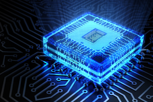
Field-programmable Gate Arrays, a brain child of Ross Freeman the cofounder of Xilinx, are essentially reprogrammable silicon chips that allow designers to create their own digital circuits unlike Application Specific Integrated Circuits.
They can be reprogrammed any time after it comes out of the US contract manufacturing company. They are typically blank slates upon which designers load bit files (configuration files / logic blocks) to achieve custom circuit designs. To map designs on a FPGA one writes some Hardware Description Language (HDL). The most common of which are VHDL and Verilog. FPGAs offer the best of two worlds by bringing two aspects together which are; the best parts of Application Specific Integrated Circuits and processor based systems.
Unlike processors, with FGPA independent processing tasks are assigned to a unique dedicated sections of the specific chip, and can as well function autonomously with less or without any influence from other logic blocks designed to increase efficiency as processing operations do not necessarily compete for the same resources. They are very good at executing parallel operations simultaneously and are ideal for high-speed and high performance operations. Components, such as multipliers increase FPGA utilization and efficiency for DSP (Digital Signal Processors) applications thereby yielding results superior to the processing abilities of the afore said (Digital Signal Processors) by breaking the process of sequential execution and achieving more clicks per cycle.
The versatility offered by FPGA means that changes can progressively be applied and replication achieved in very limited time frames, actually in a matter of hours. This serves to cover the ever changing market dynamics with minimal Nonrecurring Engineering NRE expenses and future modifications / enhancements as systems mature. minimal fabrication costs and very short lead times in assembly. It is after all, as mentioned earlier, field-upgradable.
The downside to Field-programmable Gate Arrays is that they must be configured every time power is applied as they lose their configurations every time they lose power. This is so because their configuration is stored in RAM as opposed to flash. This is however not so much of a big challenge as there are solutions in flash chips that can be employed that automatically configure up bit files at startup.
Programming of FPGA also requires familiarity with Verilog programming languages which is to many is not simple and easy to grasp. In times like this, interpreting software for LSP is advantageous.
Energy and power consumption in Field-programmable Gate Arrays is a lot more than in its contemporaries.
Design size and features are limited once a particular FPGA is chosen on the onset
Unlike with its contemporaries, cost per product goes up with increase in quantity of FPGA to be manufactured. For this reason, they are best suited for limited quantity production and prototyping.
FPGAs afford designers with a platform to design the hardware as a processor that one can write software for and customize as many serial ports as they want.
Design process for FPGAs
1. Architectural design
2. Editing
3. Compiling
Here FGPPA programming takes independent route and departs from microprocessor programming where additional synthesis process is required to produce intermediate elements that can be easily converted to different bits. This level is known as gate level logic as it is the point where logical gates of which the system will be composed are defined.
Edited files are combined logical sequences of bits are applied to control the sequencing of logical gates which are designed to accomplish particular functions as represented by assembly-language instructions. While the compiler produces bits to control fixed-gate pattern, synthesizer defines gate patterns as per the logic of the program. Output is typically in Electronic Design Interchange Format file (EDIF).
4. Linking
Bit-based outputs do not essentially control gates but must be linked to other bit patterns which eventually control logic gates, fill memory and registers. Verilog is combined to RTL netlists and synthesized to EDIF which is routed to produce HEX or TTF files that can be loaded in FPGA. It is at this point that FPGA integrates with FPGA implementable programs, places synthesized subsystems integrated into FPGA points and facilitates connections between these subsystems, enabling a seamless combined system.
5. Loading
FPGA programs (compiled, synthesized, placed, and routed) are at this level embedded in the physical FPGAs. The actual programming file may be a. HEX or TFF. Bits from this files are downloaded into the hardware in one-time proposition for nonvolatile and at-power-up proposition if otherwise.
6. Debugging programs
The program might not run smoothly at first trial and debuggers, emulators and simulators come in handy at this level to bring out points of failure
Debugging will only be achieved by simulation as FPGA does not have a fixed pattern of gates. FPGA defines the pattern of gates. The debugging is strictly done by software simulation using self-designed hardware. Debugging will be simulated with the third party programs which FPGA will integrate with in a process called test bench.
7. Delivering product
The microprocessor hardware, boards, power supplies, connections, must be correctly designed, and the software downloaded. With everything in the hardware set and in good order. FPGA design can be command-line driven or IDE-based.
FPGAs are common for their flexibility, reusability and popularity in the market. They are very quick to market as they are not preset to perform particular functions. One can get an FPGA off the shelved and easily configure it to their desired designs and reconfigure it over and over to suit diverse functions while doing away with recurrent expenses. This gives them appeal where for faster prototyping and mistakes are not catastrophic. They are best for parallelized operations and boast simple design cycles to manage and hence little manual interventions.
FPGA are most often applied in Digital Signal Radio, ASIC prototyping, Small quantity product development, Industrial control systems, high performance computing, parallel processing, Multi-Sensor Data Fusion, Crypto Investing using usd coin: usdm crypto and usdcoin wallet, Antenna beam formers for wireless communication and radar etc.
FPGAs have leaped in great steps and the number of features has grown exponentially to rival capabilities that could only have been achieved by its contemporaries. Their biggest pro is integration with third party IP and proprietary logic.